COLUMN
Jul 24, 2024
Yamamura Photonics’ LTCC development concept
Having introduced what LTCCs are in the previous article, we would now like to introduce the LTCC development concept at Yamamura Photonics.
The development of LTCCs at Yamamura Photonics began in the 1990s. It began when the LTCC business was transferred from the then parent company of Yamamura Photonics.
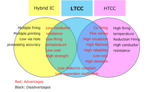
Ceramic substrates can be made smaller and thinner than standard printed circuit boards. This is because ceramic substrates can be stacked, allowing the LCR function to be designed in three dimensions. With this in mind, in the 1980s there was a growing momentum to use ceramic substrates in supercomputers to show that the same functions could be achieved in a smaller size. In this context, LTCC was developed as a ceramic-based material on which a low-cost electrode material with excellent conductive properties could be used to replace alumina substrates, which had only the expensive options of W (tungsten) and Mo (molybdenum) as conductor materials.conductor materials.
An inexpensive electrode material with excellent conductive properties is Ag (silver). However, in order to use Ag, the firing temperature has to be reduced to below 900°C. We wondered what could be done and came up with the idea of mixing aluminium oxide powder with glass powder to lower the firing temperature. By mixing with glass, in addition to lowering the sintering temperature, we were able to adjust various properties such as thermal, dielectric and mechanical properties, which broadened the range of substrate materials and led to the current product range.
Incidentally, the LTCC we developed was successfully installed in a supercomputer and launched at the time.